
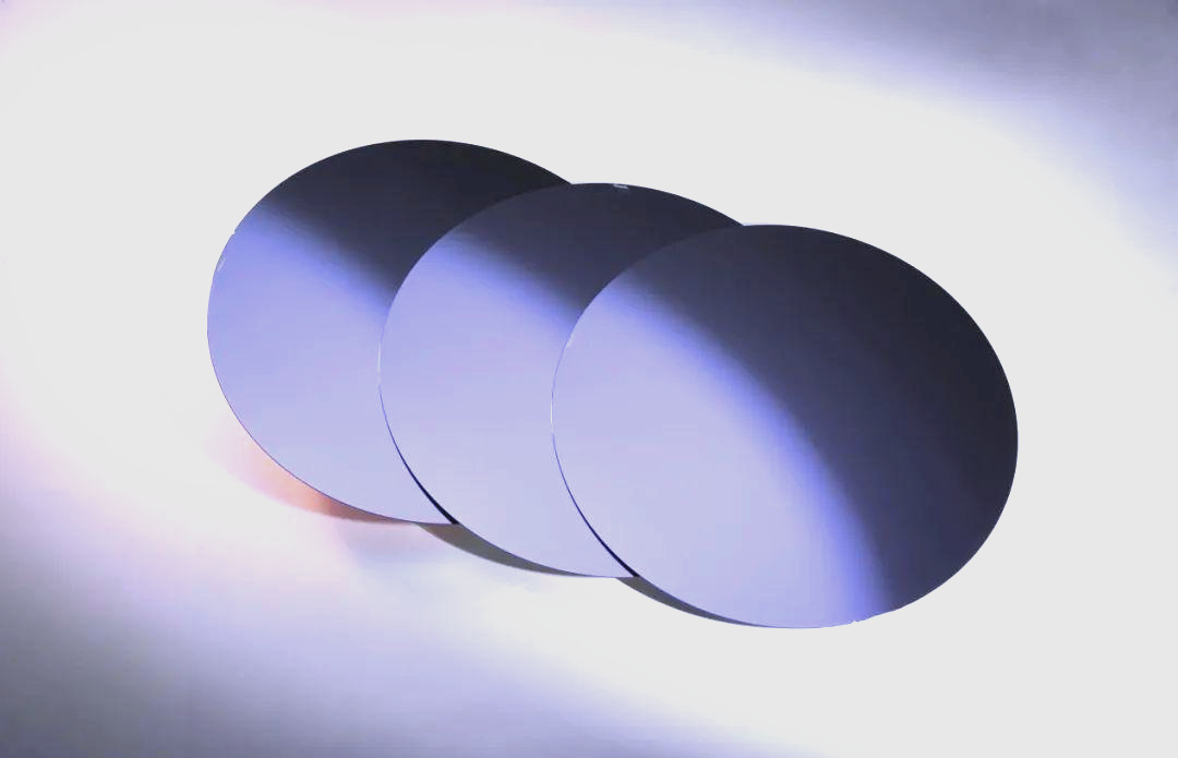
Our Silicon Carbide (SiC) Wafers
SiC Product Specifications
I. SiC Substrate
Size: 4″ / 6″ / 8″ / 12″
4-inch (100mm)
Crystal Type: 4H-SiC
Type: Semi-Insulating (SI) / N-type Conductive
Thickness: 350μm ±25μm
Semi-insulating: ≥1×10¹⁰ Ω·cm
N-type: 0.02~0.05 Ω·cm
MPD: <0.5 cm⁻² (Commercial Grade), <0.1 cm⁻² (High Grade)
6-inch (150mm)
Crystal Type: 4H-SiC
Thickness: 500μm ±25μm
Type & Resistivity:
Semi-insulating: ≥1×10¹⁰ Ω·cm
N-type Conductive: 0.02~0.05 Ω·cm
Micropipe Density: <0.05~0.1 cm⁻²
TTV: <10μm (Standard), <5μm (High Precision)
6″ N-type / 500μm / MPD<0.1 cm⁻²
6″ Semi-insulating / 500μm / MPD<0.1 cm⁻²
8-inch (200mm)
Crystal Type: 4H-SiC
Thickness: 650μm ±25μm
Type: N-type
MPD: <0.1~0.5 cm⁻²
TTV: <5μm
12-inch (300mm)
Thickness: 775μm
Type: N-type
MPD: <0.5 cm⁻²
II. SiC Epitaxial Wafer (4H-SiC)
Size: 6″ / 8″ / 12″
6-inch Epitaxial Wafer
(1) Medium & Low Voltage (650V / 1200V)
650VEpitaxial Thickness: 4~6 μm
Doping Concentration: (1.5~2.5)×10¹⁶ cm⁻³
1200VEpitaxial Thickness: 10~12 μm
Doping Concentration: (0.8~1.2)×10¹⁶ cm⁻³
Thickness Uniformity: ≤±3%
Doping Uniformity: ≤±5%
Yield: ≥96%
(2) High Voltage (1700V / 3300V)
1700V Thickness: 14~18 μm
Doping Concentration: (5~8)×10¹⁵ cm⁻³
3300V Thickness: 28~35 μm
Doping Concentration: (2~4)×10¹⁵ cm⁻³
8-inch Epitaxial Wafer
Thickness Range: 4~35 μm
Uniformity: Thickness ≤3%, Doping ≤5%
Yield: ≥96%
12-inch Epitaxial Wafer
Thickness: 10~12 μm (1200V)
Uniformity: Thickness ≤3%, Doping ≤8%