Skip to content
- Lithium niobate thin films are piezoelectric on-insulator wafers.
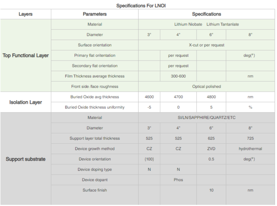
- Their stacked structure consists of a supporting substrate, which can be silicon, quartz, fused silica, sapphire, or an LN wafer,with a thermal oxide SiO₂ interlayer serving as the insulator, and the lithium niobate thin film as the functional layer atop the insulating layer.
- POI / LNOI engineered substrates enable the design of filters with high quality factor, wide bandwidth, extremely low temperature sensitivity, and low insertion loss using simple device fabrication techniques.
- These wafers are developed and used in high-speed modulators, high-Q SAW devices, infrared detectors, and terahertz devices.
- We collaborate with strategic partners experienced in smart cutting and wafer bonding technologies to provide critical piezoelectric layers for LN/LT ranging from 3″, 4″, 6″ up to 8″ in size, for the construction of special wafers with multilayer structures.